
")
")
")
")
")


In The News
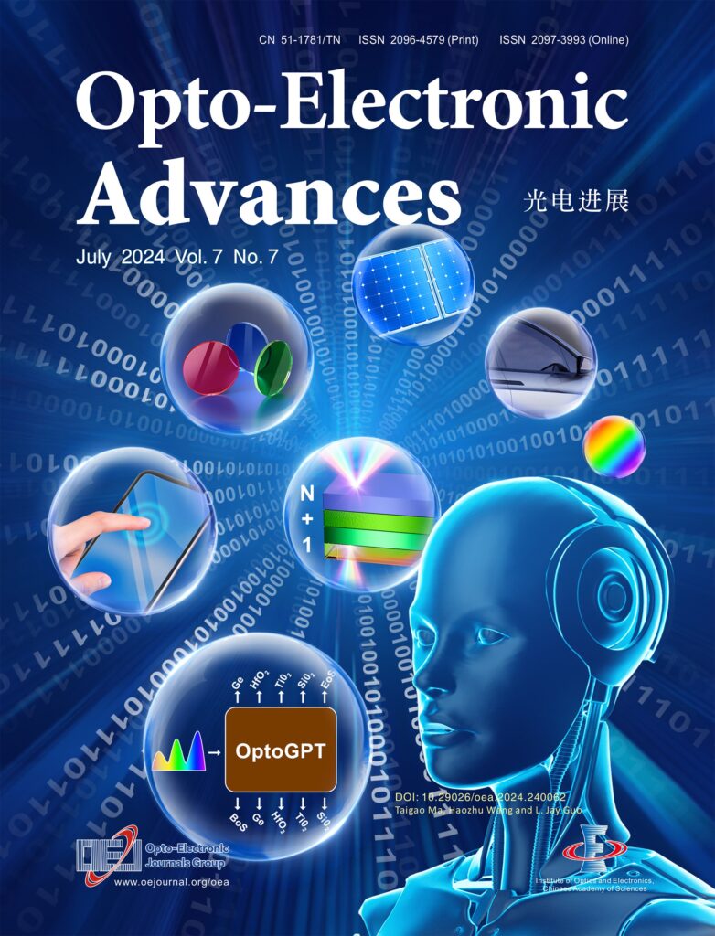
OptoGPT for improving solar cells, smart windows, telescopes and more
Optical multilayer thin film structure is one of the most important photonic structures widely used in many applications, including color filters, absorbers, optical cavities or resonators, photovoltaic and radiative cooling, special mirrors for extreme UV lithography and for space telescopes. However, the “inverse” design of multilayer structures to satisfy the desired optical response is not an easy task, considering the difficulty of co-designing material and thickness as well as the diverse types of optical responses. Here our group reports a new neural network model called OptoGPT to tackle the challenge of inverse design, with inspirations from the widely used GPT models.
In this model, we introduced “structure tokens” to denote the material and thickness information and serialize a multilayer structure into a token sequence. In this way, for arbitrary optical response, the OptoGPT model can output any type of multilayer structure, with different number of layers, different materials, and thicknesses. We further propose to design for both transmission and reflection spectrum and use multiple techniques to extend to diverse responses.
Using this model, we have successfully demonstrated a unified inverse design in different applications, including transmission filter, high reflection filter, perfect absorber, arbitrary absorber, and reflective/transmissive structural color, to name a few. Our model also works when designing different incident angles and polarization states, as well as simultaneous designs that can satisfy multiple angles and polarization requirements. Each design process is extremely fast and can be done within 0.1 seconds. This research significantly simplifies the inverse design process and sheds new light on unified design for photonic structures, making them easily accessible to researchers and engineers. (Source 1, Source 2)
Improved OLED Frees Light within Device Layers
OLEDs have become a staple in our electronic lives. Given their flexibility and low cost, they are commonly used in phones, computers and televisions. Standard OLEDs have an internal quantum efficiency of nearly 100%, meaning that in principle they almost perfectly convert energy into light. But their external quantum efficiency—the share of produced photons that escape from the device—is only around 20%.
In a typical OLED, any light that isn’t emitted at a near perpendicular angle is reflected and guided through the device. These emitted photons are lost due to internal reflections, surface-plasmon-polariton modes, and waveguide modes, which redirect and trap light. While researchers have previously reduced some light-trapping effects with intricate patterned structures, these can be costly and often interfere with the OLED’s electrical operation.
The new work adds to previous efforts by finding a way to completely eliminate light trapping due to waveguide modes without requiring an additional fabrication process. The researchers achieved this by replacing the standard transparent electrode that’s an integral part of an OLED. Instead of using the typical ITO layer, the researchers used a film of silver just 5 nm thick, deposited on a seed layer of copper.
“What I am excited about is that we have developed a very practical approach that can be easily adopted in OLED manufacturing without introducing any complicated steps,” said L. Jay Guo. (Source 1, Source 2)
Terahertz Detectors Go Handheld
The terahertz gap is a sliver between the microwave and infrared bands of the electromagnetic spectrum—the range of light’s wavelengths and frequencies. That spectrum spans from the longest, low-energy radio waves that can carry songs to our receivers to the shortest, high-energy gamma rays that are released when nuclear bombs explode and radioactive atoms decay.
In between are the microwave frequencies that can cook food or transport cell phone signals, the infrared that enables heat vision technologies, the visible wavelengths that light and color our world, and X-rays that give doctors a window under our skin.
The terahertz band is “scientifically rich,” according to Guo and colleagues. But today’s detectors either are bulky, need to be kept cold to work or can’t operate in real time. That limits their usefulness for applications like weapons and chemical detection and medical imaging and diagnosis, Guo says.
Guo and colleagues invented a special transducer that makes the light-to-sound conversion possible. A transducer turns one form of energy into another. In this case it turns terahertz light into ultrasound waves and then transmits them.
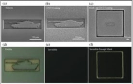
Carbon Nanotube Coating Creates ‘Perfect Black,’ Concealing 3D Objects
Researchers at the University of Michigan have developed a revolutionary carbon nanotube coating that can make three-dimensional objects appear completely flat by absorbing 99.9% of incoming light. Dubbed a “magic black cloth” by lead researcher Jay Guo, this effect is achieved by engineering the nanotube structure to have a refractive index nearly identical to that of air, eliminating reflections and scattering.
The team demonstrated this phenomenon by fabricating a microscopic silicon tank and coating it with nanotubes. Under an optical microscope, the tank seemingly vanished against a black background, appearing as a featureless dark surface. While not a full invisibility cloak, this breakthrough has exciting implications for stealth technology, ultra-high-contrast displays, and deep-space observation. Guo even speculated that a similar mechanism in space could contribute to the mystery of missing matter in the universe (Source 1, Source 2)
Published in Applied Physics Letters, this research opens new possibilities for advanced camouflage, aerospace applications, and next-generation optical materials.
Colored Decorative Solar Cells
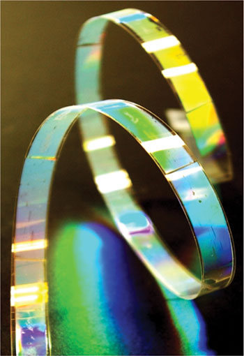
Colored, see-through solar cells invented at Michigan Engineering (guo’s lab) could enable ‘stained’ glass windows, decorative panels and even shade that makes electricity. The cells, believed to be the first semi-transparent, colored photovoltaics, have the potential to vastly broaden the use of the energy source, says Jay Guo, a professor of electrical engineering and computer science, mechanical engineering, and macromolecular science and engineering who devised them. They’re made with a technique that borrows from conventional inorganic solar cells and more up-and-coming organic cells. Their color isn’t derived from dyes, but rather from adjusting the thickness of their semiconductor layer to reflect certain wavelengths of light.
“I think this offers a very different way of utilizing solar technology rather than concentrating it in a small area,” Guo said. “We think we can make solar panels more beautiful — any color a designer wants. And we can vastly deploy these panels, even indoors.” (Source)
A Simple Filter Could Make LCDs More Efficient:
Normally, LCDs use several layers of optical devices to colorize, polarize, and shutter light from a backlight, and inefficiencies emerge at every step. Now researchers at the University of Michigan have made an optical film that promises to boost the overall efficiency of LCDs by more than 400 percent–so that 36 percent of light makes it through. The new optical film was developed by researchers led by L. Jay Guo, professor of electrical engineering and computer sciences at the university. The film colors and polarizes the light that passes through an LCD more efficiently than conventional components can. (Source)
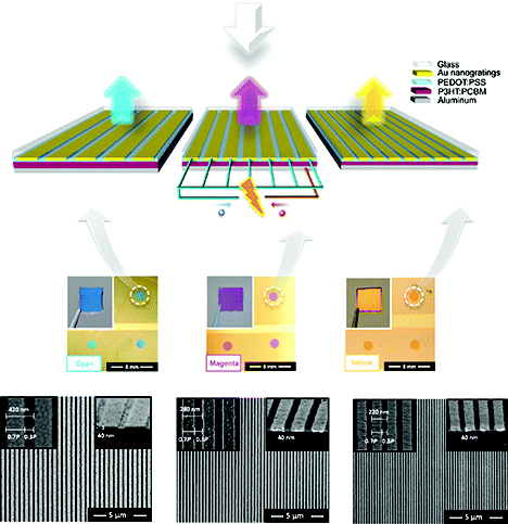
Solar Energy Harvesting of Waste Heat from Displays:
Researchers at the University of Michigan and the Chinese Academy of Science have developed a new kind of screen pixel that doubles as a solar cell and could boost the energy efficiency of cell phones and e-readers. The researchers developed a reflective photovoltaic color filter device that converts absorbed light to electricity. Reflective color filters produce visible color by absorbing certain wavelengths of light and reflecting, which is similar to the way that paint produces color. The researchers constructed filters for producing cyan, magenta, and yellow. (Source)
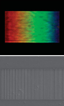
Nano Printing Goes Large:
A printing technique that could stamp out features just tens of nanometers across at industrial scale is finally moving out of the lab. The new roll-to-roll nanoimprint lithography system could be used to cheaply and efficiently churn out nano-patterned optical films to improve the performance of displays and solar cells. So far, however, it’s been difficult to scale up nanoimprint lithography reliably. To achieve the resolution needed to print transistors, for example, it’s necessary to use a flat stamp that’s a few centimeters square and must be repeatedly moved over a surface. This isn’t practical when printing large-area films for many other applications. “Displays and solar cells require printing over a much larger area and then cutting it up into sheets,” says Jay Guo, associate professor of electrical engineering and computer science at the University of Michigan. “You have to do it in a continuous fashion.” (Source)
Big and Bright Flexible Display:
Organic light-emitting diode (OLED) displays are attractive because they are bright, efficient, and thin enough to be flexible. But they are currently limited to use in small displays, such as those in mobile phones. That’s partly due to the failings of one piece of the device, a transparent electrode used to light up the display. Now researchers at the University of Michigan have developed a new type of electrode that could help clear the way for large, flexible OLED displays. The new electrode is a grid of highly conductive metal wires so thin that they are essentially transparent. Electrical-engineering and computer-science professor L. Jay Guo says that the electrode should be more flexible and less expensive than ITO, while not degrading the organic materials. (Source)